NextGen VLSI Design Lab - 1 Day course in Sacramento, CA
Schedule
Fri, 12 Dec, 2025 at 09:00 am to Fri, 12 Jun, 2026 at 05:00 pm
UTC-08:00Location
Regus - Sacramento, 8880 Cal Centre | Sacramento, CA

About this Event
Group Discounts:
Save 10% when registering 3 or more participants
Save 15% when registering 10 or more participants
About the course:
Duration: 1 Full Day (8 Hours)
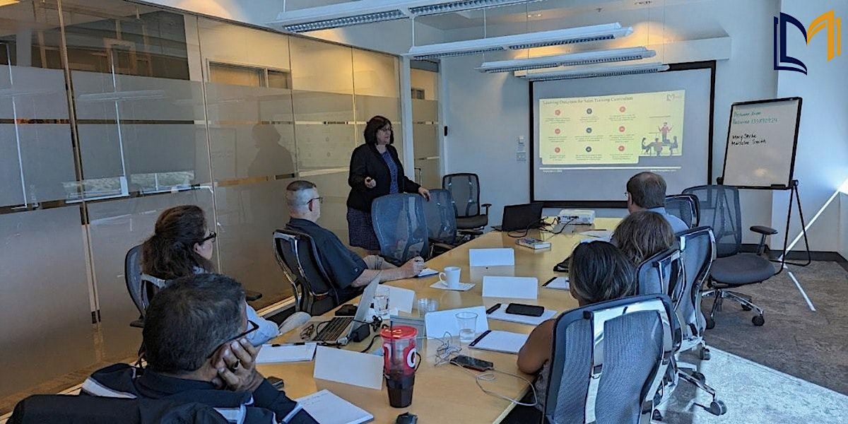
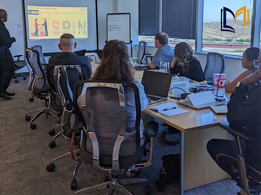
Delivery Mode: Classroom (In-Person)
Language: English
Credits: 8 PDUs / Training Hours
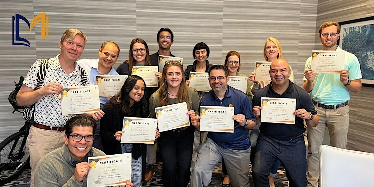
Certification: Course Completion Certificate
Refreshments: Lunch, Snacks and beverages will be provided during the session
Course Overview:
This one‑day course offers a focused dive into the principles and practices of Very Large‑Scale Integration (VLSI) design, covering system‑on‑chip architectures, logic design, timing, physical implementation and verification flows. Participants will explore why VLSI is critical in modern electronics—from mobile devices through to automotive and industrial applications—and how to efficiently design and optimize complex integrated circuits for performance, power and area.
Learning Objectives:
By the end of this course, you will:
- Understand the end to end VLSI design flow: specification → RTL design → synthesis → place & route → verification
- Gain insight into logic design considerations, timing closure and physical constraints in advanced process nodes
- Explore power, performance and area trade offs in VLSI and how to make informed architecture/design decisions
- Learn key verification strategies and techniques to ensure functional correctness and design robustness
- Examine real world design challenges in system on‐chip (SoC) integration, IP reuse, and design for testability
- Discover best practices for interfacing with fabrication, layout aware design, and leveraging physical implementation feedback
- Acquire actionable tools and methodologies that can be applied immediately to your next VLSI design or project
Who can Attend?
This course is designed for engineers, VLSI design professionals, FPGA/ASIC designers, verification engineers, systems architects, technical team leads and managers involved in semiconductor or embedded electronics development who wish to strengthen their VLSI design knowledge and apply industry best practices.
Why Choose this Course?
Our VLSI Design course is delivered by globally recognized corporate training experts, led by certified instructors with real‑world experience in semiconductor design and embedded systems. You benefit from interactive classroom learning, practical insights drawn from live industry case studies, and proven methodologies that translate directly into improved design efficiency and project success. Choose this training to elevate your team’s capabilities, stay ahead of design‑innovation trends and deliver competitive advantage in a fast‑evolving electronics market.
©2025 Mangates Tech Solutions Pvt Ltd. This content is protected by copyright law. Copy or Reproduction without permission is prohibited.
Our Royalty Referral Program
Know a team or professional who could benefit from our workshops? Refer them and earn attractive royalties for every successful registration.
For royalty-related queries, contact [email protected]
Want to train your entire team?
In-House sessions are available for organizations covering the complete chip design flow from specification to verification, emphasizing hands-on practice with logic, timing, physical design, SoC integration, and verification. It equips engineering teams with practical skills in EDA tools, design optimization, and workflow efficiency to deliver high-performance, reliable VLSI designs.
📧 Contact us today to schedule a customized in-house session:
Agenda
Module 1: Course Introduction & VLSI Overview
Info:
• Overview of VLSI and semiconductor industry trends
• Importance of VLSI in modern electronics and embedded systems
• Key challenges and opportunities in VLSI design
Module 2: VLSI Design Flow Fundamentals
Info:
• End-to-end design flow: Specification → RTL → Synthesis → Place & Route → Verification
• Roles and responsibilities in each stage
• Real-world examples of design flow application
Module 3: Logic Design & Timing Analysis
Info:
• Combinational and sequential logic design techniques
• Timing constraints, timing closure, and timing optimization
• Power, performance, and area (PPA) considerations
Module 4: Physical Design & Implementation
Info:
• Floor planning, placement, routing, and optimization
• Design for manufacturability (DFM) and design for testability (DFT)
• Handling process technology nodes and layout-aware design
Module 5: Verification & Validation
Info:
• Functional verification strategies
• Simulation, static and formal verification methods
• Case studies from real ASIC/FPGA projects
Module 6: Advanced VLSI Topics & SoC Integration
Info:
• System-on-Chip design considerations
• IP reuse strategies and integration challenges
• Power management, clock domain crossing, and signal integrity
Module 7: Tools & Methodologies
Info:
• Overview of commonly used VLSI tools for design, simulation, and verification
• Practical tips for workflow optimization and efficiency
Module 8: Q&A, Wrap-Up & Key Takeaways
Info:
• Summary of concepts learned
• Open discussion on practical applications in participants’ projects
• Distribution of course completion certificates
Where is it happening?
Regus - Sacramento, 8880 Cal Centre, 8880 Cal Center Drive #4th Floor, Sacramento, United StatesEvent Location & Nearby Stays:
USD 514.07 to USD 674.80